Monday, 27 August 2012

EUV

Extreme UV:

1)Found from some semiconductor blog. Gives good idea about the device scaling and the issues.

EUV is the great hope for avoiding having to go to triple (and more) patterning if we have to stick with 193nm light. There were several presentations at Semicon about the status of EUV. Here I'll discuss the issues with EUV lithography and in a separate post discuss the issues about making masks for EUV.

It is probably worth being explicit and pointing out that the big advantage of EUV, if and when it works, is it is single patterning technology (for the forseeable future) with just one mask and one photolithography process per layer.

First up was Stephan Wurm, the director of litho for Sematech (it's their 25th anniversary this year, seems like only yesterday...). He talked about where EUV is today. Just a little background about why EUV is so difficult. First, at these wavelengths, the photons won't go through lenses or even air. So we have to switch from refractive optics (lenses) to reflective optics (mirrors) and put everything in a vacuum. The masks have to be reflective too but I'll talk about that in the next blog. Obviously we need a different photoresist than we use for 193nm. And, most critically, we need a light source that generates EUV light (which is around 14nm wavelength, so by the time EUV is inserted into production it will already be close to the feature size but we've got pretty good at making small features with long wavelength light).

The status of the resist is that we now have chemically amplified resist (CAR) with adequate resolution for a 22nm half pitch (22nm lines with 22nm spaces) and seems to be OK down to 15nm. A big issue is sensitivity, it takes too much light to expose the resist which reduces throughput. However, when we have had sensitivity problems in the past they were not so severe and were solved earlier. Line width roughness (LWR) continues to be a problem and will need to be solved with non-lithographic cleanup. Contact holes continue to be a problem. Stephan discussed mask blank defect and yield issues but, as I said, that comes in the next blog.

Next up was Hans Meiling from ASML (with wads of Intel money sticking out of his back pocket). They have already shipped 6 NXE-3100 pre-production tools to customers for them to start doing technology development. They have 7 3300 scanners being built.

You can't get EUV out of a substance in its normal state, you need a plasma. So you don't just plug in an EUV bulb like you do for visible light. You take little droplets of tin, zap them with a very high powered CO2 laser, and get a brief flash of light. They have run sources like this for 5.5 hours continuously. It takes a power input of 30kW to get 30W of EUV light, so not the most efficient process.

Contamination of mirrors is one challenge, given that putting everything in a vacuum and using metal plasma is how we make interconnect and for sure we don't want to coat our mirrors with tin. ASML found problems with the collecting optics not staying clean after 10M pulses, which sounds a lot until you realize it is about 1 week of operation in a fab running the machine continuously. They now have 3 or 4 times more but there is clearly progress to be made.

Reflectivity of the mirrors is a problem. These are not the sort of mirror you have in your bathroom, they are Mo/Si multilayers which forms a Bragg reflectorthat reflects light due to multilayer interference. Even with really good mirrors, only about 70% of the EUV light is reflected from the mirror and since the optics require 8 or more mirrors to focus the light first on the mask and then on the wafer, very little of the light you start with (maybe 4%) ends up hitting the photoresist. Some of these mirrors are grazing incidence mirrors, which are mirrors that bend the light along their length like some pinball machine bending the path of the ball and can be used to focus a beam.

Currently they are managing to get 5-7W and have demonstrated up to 30W. For high throughput the source needs to be 200W so this is still something that seems out of reach from just tweaking the current technology. 

The light source power issue is the biggest issue in building a high-volume EUV stepper. Intel is betting that a few billion dollars and ASML will solve it.
double patterning

Refer below:

1)http://www.techdesignforums.com/eda/guides/double-patterning/

2)Taken from one of the semiconductor blog in quotes below:
"Cadence has a new white paper out about the changes in IC design that are coming at 20nm. One thing is very clear: 20nm is not simply "more of the same". All design, from basic standard cells up to huge SoCs has several new challenges to go along with all the old ones that we had at 45nm and 28nm.

I should emphasize that the paper is really about the problems of 20nm design and not a sales pitch for Cadence. I could be wrong but I don't think it mentions a single Cadence tool. You don't need to be a Cadence customer to profit from reading it.

The biggest change, and the one that everyone has heard the most about, is double patterning. This means that for those layers that are double patterned (the fine pitch ones) two masks are required. Half the polygons on the layer go on one mask and the other half on the other mask. The challenge is that no patterns on either mask can be too close, and so during design the tools need to ensure that it is always possible to divide the polygons into two sets (so, for example, you can never have three polygons that are minimum distance from each other at any point, since there is no way to split them legally into two). Since this is algorithmically a graph-coloring problem this is often referred to as coloring the polygons.


Place and route obviously needs to be double pattern aware and not create routing structures that are not manufacturable. Less obvious is that even if standard cells are double pattern legal, when they are placed next to each other they may cause issues between polygons internal to the cells.

Some layers at 20nm will require 3 masks, two to lay down the double patterned grid and then a third "cut mask" to split up some of the patterns in a way that wouldn't have been possible to manufacture otherwise.

Another issue with double patterning is that most patterning is not self-aligned, meaning that there is variation between polygons on the two masks that is greater than the variation between two polygons on the same mask (which are self-aligned by definition). This means that verification tools need to be aware of the patterning and, in some cases, designers need to be given tools to assign polygons to masks where it is important that they end up on the same mask.


Design rules at 20nm are incredibly complicated. Cadence reckon that of 5,000 design rules only 30-40 are for double patterning. There are layout direction orientation rules, and even voltage dependent design rules. Early experience of people I've talked to is that the design rule are now beyond human comprehension and you need to have the DRC running essentially continuously while doing layout.

The other big issue with 20nm are layout dependent effects (LDEs). The peformance of a transistor or a gate no longer depends just on its layout in isolation but also on what is near it. Almost every line on the layout such as the edge of a well has some non local effect on the silicon causing performance changes in active areas nearby. At 20nm the performance can vary by as much as 30% depending on the layout context.

A major cause of LDEs is mechanical stress. Traditionally this was addressed by guardbanding critical paths but at 20nm this will cause too much performance loss and instead all physical design and analysis tools will need to be LDE aware.

Of course in addition to these two big new issues (double patterning, LDEs) there are all the old issues that just get worse, whether design complexity, clock tree synthesis and so on.

Based on numbers from Handel Jones's IBS, 20nm fabs will cost from $4-7B (depending on capacity), process R&D will be $2.1-3B on top of that, and mask costs will range from $5-8M per design. And design costs: $120-500M. You'd better want a lot of die when you get to production."


SSTA

Product binning

Product binning can be done based on many operational parameters like voltage, freq., disabling some IPs, operating temperature, etc. Purpose is to increase the yield. Below link gives some basic idea about product binning:

http://en.wikipedia.org/wiki/Product_binning

http://ieeexplore.ieee.org/xpl/login.jsp?tp=&arnumber=6212859&url=http%3A%2F%2Fieeexplore.ieee.org%2Fxpls%2Fabs_all.jsp%3Farnumber%3D6212859

Wednesday, 22 August 2012

Logic Synthesis

What is Logic Synthesis ?


“ Logic synthesis is the process of converting a high-level description of the design into an optimized gate-level  representation, given a standard cell library and certain design constraints “

Why Perform Logic Synthesis ?


1. Automatically manages many details of the design process:

• Fewer bugs

• Improves productivity 


2.  Abstracts the design data (HDL description) from any particular implementation technology

• Designs can be re-synthesized targeting different chip technologies;

E.g.: first implement in FPGA then later in ASIC


3. In some cases, leads to a more optimal design than could be

achieved by manual means (e.g.: logic optimization) 


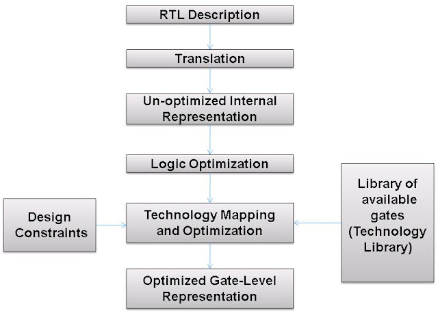
Logic Synthesis Flow : RTL TO GATES


RTL description:

Design at a high level using RTL constructs.


Translation:

Synthesis Tool convert the RTL description to un-optimized Internal representation.(Boolean form)


Un-optimized Intermediate Representation:

Represented internally by the logic synthesis tool in terms of Internal data structure.


Logic Optimization:

Logic is optimized to remove redundant logic.

Technology Mapping and Optimization:

The synthesis tool takes the internal representation and implements the representation in gates, using the cells provided in the technology library.


Technology Library:

library cells that can be basic gates or macro cells.


The cell description contains information about the following:


• Functionality of the cell.

• Area of the cell layout.

• Timing information about the cell.

• Power information about the cell.


Design Constraints:

1.Area:

  • Designer can specify area constraint and synthesis tool will optimize for minimum area. 
  • Area can be optimized by having lesser number of cells and by replacing multiple cells with single cell that includes both functionality. 

2. Timing:

  • Designer specifies maximum delay between primary input and primary output.
There are three types of critical paths:
I.Path between a primary input and primary output.
II.Path from any primary input to a register.
III.Path from a register to a primary output.
IV.Path from a register to another register


3. Power:

  • Development of hand-held devices has led to reduction of battery size and hence low power consuming systems..


Points to note about synthesis 


  • For very big circuits, vendor technology libraries may yield non- optimal result. 
  • Translation, logic optimization and technology mapping are done internally in the logic synthesis tool and are not visible to the designer. 
  • Timing analyzer built into synthesis tools will have to account for interconnect delays in the total delay calculation


Saturday, 18 August 2012

Timing Optimization Techniques


Timing Optimization Techniques are as follows:

1.Mapping :

Mapping converts primitive logic cells found in a netlist to technology-specific logic gates found in the library on the timing critical paths.

2. Unmapping:
Unmapping converts the technology-specific logic gates in the netlist to primitive logic gates on the timing critical paths.

3. Pin Swapping :
Pin swapping optimization examines the slacks on the inputs of the gates on worst timing paths and optimizes the timing by swapping nets attached to the input pins, so the net with the least amount of slack is put on the fastest path through the gate without changing the function of the logic.

4. Buffering:

Buffers are inserted in the design to drive a load that is too large for a logic cell to efficiently drive.
If the net is too long then the net is broken and buffers are inserted to improve the transition which will ultimately improve the timing on data path and reduce the setup violation.
To reduce the hold violations buffers are inserted to add delay on data paths.

5. Cell Sizing

Cell sizing is the process of assigning a drive strength for a specific cell in the library to a cell instance in the design.If there is a low drive strength cell in the timing critical path then this cell is replaced by higher drive strength cell to reduce the timing violation.

6. Cloning :

Cell cloning is a method of optimization that decreases the load of a very heavily loaded cell by replicating the cell. Replication is done by connecting an identical cell to the same inputs as the original cell.Cloning clones the cell to divide the fanout load to improve the timing.

7. Logic Restructuring

Logic restructuring means to rearrange logic to meet timing constraints on critical paths of design.

Advanced OCV

What is Advanced OCV -

AOCV uses intelligent techniques for context specific derating instead of a single global derate value, thus reducing the excessive design margins and leading to fewer timing violations. This represents a more realistic and practical method of margining, alleviating the concerns of overdesign, reduced design performance, and longer timing closure cycles.
Advanced OCV  determines derate values as a function of logic depth and/or cell, and net location. These two variables provide further granularity to the margining methodology by determining how much a specific path in a design is impacted by the process variation.

There are two kinds of variations.
1) Random Variation
2) Systematic Variation

Random Variation-
Random variation is proportional to the logic depth of each path being analyzed.
The random component of variation occurs from lot-to-lot, wafer-to-wafer, on-die and die-to-die. Examples random variation are variations in gate-oxide thickness, implant doses, and metal or dielectric thickness.


Systematic Variation-
Systematic variation is proportional to the cell location of the path being analyzed.
The systematic component of variation is predicted from the location on the wafer or the nature of the surrounding patterns. These variations relate to proximity effects, density effects, and the relative distance of devices. Examples of systematic variation are variations in gate length or width and interconnect width.

Take the example of random variation, given the buffer chain shown in Figure 1, with nominal cell delay of 20, nominal path delay @ stage N = N * 20. In a traditional OCV approach, timing derates are applied to scale the path delay by a fixed percentage, set_timing_derate late 1.2; set_timing_derate early 0.8


Figure 1: Depth-Based Statistical Analysis
 Statistical analysis shows that the random variation is less for deeper timing paths and not all cells are simultaneously fast or slow. Using statistical HSPICE models, Monte-Carlo analysis can be performed to measure the accurate delay variation at each stage. Advanced OCV derate factors can then be computed as a function of cell depth to apply accurate, less pessimistic margins to the path.

Figure 2a shows an example of how PrimeTime Advanced OCV would determine the path depth for both launch and capture. These values index the derate table, as shown in Figure 7, to select the appropriate derate values.
                                  Fig 2a-Depth Based Advanced OCV


Effects of systematic variation shows that paths comprised of cells in close proximity exhibit less variation relative to one another. Using silicon data from test-chips, Advanced OCV derate factors based on relative cell-location are then applied to further improve accuracy and reduce pessimism on the path. Advanced OCV computes the length of the diagonal of the bounding box, as shown in Figure 2b, to select the appropriate derate value from the table.


Fig2b -Distance Based advanced OCV


PrimeTime Advanced OCV Flow -
PrimeTime internally computes depth and distance metrics for every cell arc and net arc in the design. It picks the conservative values of depth and distance thus bounding the worst-case path through a cell.

Fig-3

Low Power design


Special Cells

Special Cells

Here are the description of the cells used during Physical design.


  • Tap cells
  • Tie cells


  • Tie-high and Tie-Low cells are used to connect the gate of the transistor to either power or ground.In Lower technology nodes, if the gate is connected to power/ground the transistor might be turned on/off due to power or ground bounce
    These cells are part of standard-cell library
    The cells which require Vdd (Typically constant signals tied to 1) connect to Tie high cells
    The cells which require Vss/Gnd (Typically constant signals tied to 0) connect to Tie Low cells

  • Endcap cells
  • Decap cells.


I
n cross coupled design (Figure A), the drain of the PMOS connects to the gate of the NMOS, whereas the drain of the NMOS is tied to the gate of the PMOS.Both transistors in this design are still in the linear region. In the standard decap design, the gates of the transistors are directly connected to either VDD or VSS, depending on the transistor type. In this case, the gate of the NMOS device is connected to VDD through the channel resistance of the PMOS device. Similarly, the gate of the PMOS device is tied the channel resistance of the NMOS device and then connected to VSS. The added channel resistance to the gate provides the input resistance  Rin for ESD protection. The input resistance can help to limit the maximum current flow to the decap so that the voltage seen from the gate of the decap is also limited
  • Spare cellsSpare cells are extra cells placed at regular interval in the chip. They are floating cells and they are placed in a group of functional cells like(and, or, nor, mux, flop, inverter, buffer).
    Once the chip is taped out and if any functional issue is found or any feature enhancement is required, these pre-placed cells can be used to add functionality without redoing the entire design.In these cased only the metal-ecos are performed and all the base layers are untouched, thus saving the cost of manufacturing.
    Some companies are using the Post mask Eco cells( special kind of cells which can be programmed to function as any gate) in their design. when not used they act as simple filler cells.
    If any design changes are required then these cells can be used to perform the functionality.Spare cells inputs are connected to Ground/Power when they are placed in the design and their outputs are left floating, if they are required to be used then their inputs are disconnected from VDD/GND and connected to functional logic in ECO mode.
    Spare cells are categorized mainly in two forms:
    Combinational:
    They are generally added by PNR tools and can be added using scripts in the floorplan or placement stages.
    Sequential:
    They are generally added in the RTL itself so that they can be stitched in the scan chain for testability purpose
  • Tap cells


Latch up violation


Latch up in CMOS


Please refere the below link on Wikipedia for detailed explanation of Latch up.

Latch up problem in CMOS


Friday, 17 August 2012

Crosstalk


Definition

When 2 wire segments are in close proximity they interact with each other electrically, this is on account of coupling capacitor between these 2 nets.This Phenomenon is called crosstalk.
This coupling capacitor causes crosstalk delay and crosstalk noise.

Crosstalk Delay:

If there is a significant amount of crosstalk between 2 wire segments and both the nets switch(in the same or opposite) direction simultaneously then it results in crosstalk delay.Crosstalk delay can cause setup and hold violations.
I leave it to the imagintion of the reader to figure out how this happens.

Crosstalk Noise:


If one net is static and a nearby net rapidly switches,owing to coupling capacitance between these 2 wires we will see a glitch on the static net and this is crosstalk noise.

Electromigration

Electromigration (EM) is generally considered to be the result of momentum transfer from the electrons due to high current density. Atoms get displaced from their original position causing voids(opens) & hillocks(shorts) in the metal layer


Joule heating also accelerates EM because higher temperatures cause a higher number of metal ions to diffuse. Under extreme joule heating, melting can occur. 


EM causing opens                           EM causing shorts


Cell EM 

Cell EM rules address the EM caused by current within a cell. Cell EM rules operate on the principle that, although the currents within a cell cannot be calculated due to a lack of physical layout information, they can be controlled based on external physical entities.The tool estimates the detrimental effects of currents within a cell as a function of its:

• Output load

• Input slew

• Switching frequency

Wire EM


There are two types of wire EM:

Signal EM -- It is performed net by net ,simulating the charging and discharging for all possible paths to determine the worst case average and rms current for each wire segment.Once currents are determined ,current density is computed.

Power EM -- EM effects produced on power nets is noted as power EM

Techniques to solve EM:

1) Increase the width of the wire

2) Buffer insertion

3) Upsize the driver

4) Switch the net to higher metal layer


Clock Tree Synthesis

Some Basic STA Terminologies to understand CTS effectively

Skew is the difference in arrival of clock at two consecutive pins of a sequential element.

Positive skew- If capture clockcomes late than launch clock then it is called positive skew. 

Negative skew-If capture clock comes early than launch clock it is called –ve skew. 

Local skew- It is the difference in arrival of clock at two consecutive pins of a sequential element. 

Global skew- It is Defined as the difference between max insertion delay and the min insertion delay of any flops. 

Boundary skew-It is defined as the difference between max insertion delay and the min insertion delay of boundary flops. 

Useful skew-If clock is skewed intentionally to resolve violations, it is called useful skew.

Latency- Latency is the delay of the clock source and clock network delay.

Source latency- The delay from the clock origin point to the clock definition point in the design.

Network latency- The delay from the clock definition point to the clock pin of the register.

Uncertainity- Clock uncertainty is the time difference between the arrivals of clock signals at registers in one clock domain or between domains.

Basically it is the margin including skew and jitter

Jitter- Jitter is the short-term variations of a signal with respect to its ideal position in time.

It is the variation of the clock period from edge to edge.

What is CTS

CTS basically develops the interconnect that connect the system clock to all the cells in the chip.

When CTS

CTS is performed after placement as after placement stage only all the standard cells are legalized.

Why CTS

CTS is performed after placement as after placement stage only all the standard cells are legalized.

Mainly the goals of CTS are :

1)Minimizing Clock skew
2)Minimizing Insertion delay
3)Minimizing power dissipation

Inputs required for CTS:

-- Detailed placement database
-- Target for latency and skew if specified

-- Buffers or Inverters (specific) for building the clock tree

Output:

Database with properly build clock tree in the design

Checklist after CTS:

-- Timing Reports for setup and hold

-- Clock tree report

-- Skew report
-- Power & Area report


Static Timing Analysis


STA Basics


Static Timing Analysis

Static timing analysis is a method of validating the timing performance of a design by checking all possible paths for timing violations without having to simulate .
No vector generation is required ,no functionality check is done


Why is timing analysis important when designing a chip?


Timing is important because just designing the chip is not enough; we need to knowhow fast the chip is going to run, how fast the chip is going to interact with the otherchips, how fast the input reaches the output etc…Timing Analysis is a method of verifying the timing performance of a design bychecking for all possible timing violations in all possible paths.

Why do we normally do Static Timing Analysis and not Dynamic Timing Analysis? What is the difference between them?


Timing Analysis can be done in both ways; static as well as dynamic. Dynamic Timing analysis requires a comprehensive set of input vectors to check the timing characteristics of the paths in the design. Basically it determines the full behavior of thecircuit for a given set of input vectors. Dynamic simulation can verify the functionality of the design as well as timing requirements. For example if we have 100 inputs then weneed to do 2 to the power of 100 simulations to complete the analysis. The amount of analysis is astronomical compared to static analysis.Static Timing analysis checks every path in the design for timing violations withoutchecking the functionality of the design. This way, one can do timing and functionalanalysis same time but separately. This is faster than dynamic timing simulation becausethere is no need to generate any kind of test vectors. That’s why STA is the most popularway of doing timing analysis


Dynamic Vs Static STA


Basic Definitions


* clock :  It is a signal in the design in respect to which all other signals are synchronized. There can be multiple clocks in design.

1) Setup Time:

  • Setup time is the minimum amount of time the data signal should be held steady before the clock event so that the data are reliably sampled by the clock. This applies to synchronous circuits such as the flip-flop. 
  •  In short I can say that the amount of time the Synchronous input (D) must be stable before the active edge of the Clock. 
  • The Time when input data is available and stable before the clock pulse is applied is called Setup time.


2) Hold time:

  • Hold time is the minimum amount of time the data signal should be held steady after the clock event so that the data are reliably sampled. This applies to synchronous circuits such as the flip-flop. 
  • Or in short I can say that the amount of time the synchronous input (D) must be stable after the active edge of clock. 
  • The Time after clock pulse where data input is held stable is called hold time.


3) Slack: 

  • It is difference between the desired arrival times and the actual arrival time for a signal. 
  • Slack time determines [for a timing path], if the design is working at the desired frequency. 
  • Positive Slack indicates that the design is meeting the timing and still it can be improved. 
  • Zero slack means that the design is critically working at the desired frequency. 
  • Negative slack means , design has not achieved the specified timings at the specified frequency. 
  • Slack has to be positive always and negative slack indicates a violation in timing.

4) Required time: 

The time within which data is required to arrive at some internal node of the design. Designer specify this value by setting constraints.

5) Arrival Time: 

The time in which data arrives at the internal node. It incorporates all the net and logic delays in between the reference input point and the destination node. 

 Setup Slack = Required time - Arrival time
 Hold slack = Arrival time - Required time 

6) Setup Slack: 

Amount of margin by which setup requirements are met.


TCL = Total combinational delay in a pipe-lined stage


TRC = RC delay of interconnects


TC-Q = Clock to output delay


Tarrival = Arrival time (at node)


Tcycle,min = Minimum Achievable clock cycle


To meet the setup requirements the following equation must be satisfied.


Tslack,setup = Tcycle – Tarrival - Tsetup (For all Paths )

Here Tarrival= TCL + TRC + TC-Q

7) Hold Slack: 


Amount of margin by which hold time requirements are met.


Tarrival >= Thold


Tarrival – Thold = Thold,slack


Thold,slack = TCL + TRC + TC-Q - Thold

  • The Negative value of Hold Slack means signal value propagates from one register to next, too fast that it overrides the old value before that can be detected by the corresponding active clock edge. 
  • The Clock frequency variation doesn’t effects the Hold time or the Hold slack so it is critical to fix the Hold time violations in a design prior to the setup violation if both exists simultaneously


8) Clock jitter: 


Clock jitter is the amount of cycle-to-cycle variation that can occur in a clock’s period. Because clocks are generated by real physical devices such as phase-locked loops, there is some uncertainty, and a perfect waveform with an exact period of x nanoseconds cannot be achieved. 


9) Source latency: 

The delay from the clock origin point to the clock definition point in the design.
It is the insertion delay external to the circuit which we are timing. It applies to only primary clocks.


10) Network Latency: 

The delay from the clock definition point to the clock pin of the register
It is the internal delay for the circuit which we are timing (the delay of the clock tree from the source of the clock to all of the clock sinks).


11)I/O latency

If the flop of the block is talking with another flop outside the block, clock latency (network) of that flop will be the i/o latency of the block.


12)Clock Skew: 


It is the difference in arrival times of the capture edge at two adjacent Flip-flop pairs.

13) Positive skew

 If capture clock comes late than launch clock then it is called positive skew.


14) Negative skew

If capture clock comes early than launch clock it is called –ve skew.


15)Local skew-

 It is the difference in arrival of clock at two consecutive pins of a sequential element.

16) Global skew-

It is Defined as the difference between max insertion delay and the min insertion delay of any flops.
It is also defined as the difference between shortest clock path delay and longest clock path delay reaching two sequential elements


17) Boundary skew-

It is defined as the difference between max insertion delay and the min insertion delay of boundary flops.


18)Useful skew-

If clock is skewed intentionally to resolve violations, it is called useful skew.


19) Recovery and Removal Time

These are timing checks for asynchronous signals similar to the setup and hold checks.
Recovery time is the minimum amount of time required between the release of an asynchronous signal from the active state to the next active clock edge.
Example: The time between the reset and clock transitions for a flip-flop. If the active edge occurs too soon after the release of the reset, the state of the flip-flop can be unknown.
Removal time specifies the minimum amount of time between an active clock edge and the release of an asynchronous control signal.
The following diagram illustrates recovery and removal times for an active low reset signal (RESET_N) and positive-edge triggered  CLOCK


Timing Paths

The different kinds of paths when checking the timing of a design are as follows.

1. Input ports/pin --> Sequential element (Register).
2. Sequential element (Register) --> Sequential element (Register)
3. Sequential element (Register) --> Output Pin/Port
4. Input ports/pin -->  Output Pin/Port


The static timing analysis tool performs the timing analysis in the following way.
  1. STA Tool breaks the design down into a set of timing paths. 
  2. Calculates the propagation delay along each path. 
  3. Checks for timing violations (depending on the constraints e.g. clock) on the different paths and also at the input/output interface.


    Timing Analysis is performed by splitting the design into different paths based on: 


    • Start Points 
    • End points  

    • Start points comprise of:
      A clock, a primary input port, a sequential cell, a clock input pin of a sequential cell, a data pin of a level-sensitive latch, or a pin that has an input delay specified.
    • End points comprise of:
      A clock, a primary output port, a sequential cell, a data input pin of a sequential cell, or a pin that has an output delay specified. 

    Calculation of the propagation delay along each path:

    STA calculates the delay along each timing path by determining the Gate delay and Net delay.

    1. Gate Delay : Amount of delay from the input to the output of a logic gate. It is calculated based on 2 parameters.

    ---Input Transition Time 
    ---Output Load Capacitance

    2. Net Delay : Amount of delay from the output of a gate to the input of the next gate in a timing path. It depends on the following parameters.

    --Parasitic Capacitance.
    --Resistance of net 

    During STA, the tool calculates timing of the path by calculating:
    1. Delay from input to output of the gate (Gate Delay).
    2. Output Transition Time -> (which in turn depends on Input Transition Time and Output Load Capacitance)

    Timing Exceptions 

    Timing exceptions are nothing but constraints which don’t follow the default when doing timing analysis. The different kinds of timing exceptions are

    1. False path: If any path does not affect the output and does not contribute to the delay of the circuit then that path is called false path.

    2. Multi-cycle Path : Multicycle paths in a design are the paths that require more than one clock cycle. Therefore they require special Multicycle setup and hold-time calculations

    3. Min/Max Path : This path must match a delay constraint that matches a specific value. It is not an integer like the multicycle path. For example:Delay from one point to another max: 1.67ns; min: 1.87ns

    4. Disabled Timing Arcs : The input to the output arc in a gate is disabled.
     For e.g. 3 input and gate (a, b, c) and output (out). If you want you can disable the path from input ‘a’ to output ‘out’ using disable timing arc constraint.

    Clock Path:

    Please check the following figure:


    In the above fig its very clear that for clock path the starts from the input port/pin of the design which is specific for the Clock input and the end point is the clock pin of a sequential element. In between the Start point and the end point there may be lots of Buffers/Inverters/clock divider.

    Clock Gating Path:


    Clock path may be passed trough a “gated element” to achieve additional advantages. In this case, characteristics and definitions of the clock change accordingly. We call this type of clock path as “gated clock path”.
    As in the following fig you can see that

    LD pin is not a part of any clock but it is using for gating the original CLK signal. Such type of paths are neither a part of Clock path nor of Data Path because as per the Start Point and End Point definition of these paths, its different. So such type of paths are part of Clock gating path.

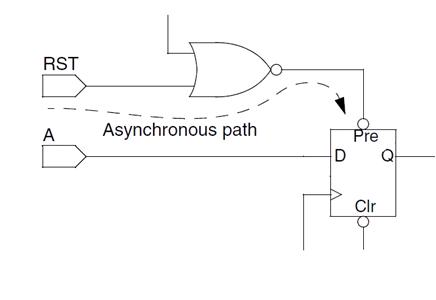
    Asynchronous path:

    A path from an input port to an asynchronous set or clear pin of a sequential element. 
    See the following fig for understanding clearly.


    As you know that the functionality of set/reset pin is independent from the clock edge. Its level triggered pins and can start functioning at any time of data. So in other way we can say that this path is not in synchronous with the rest of the circuit and that's the reason we are saying such type of path an Asynchronous path.


    Antenna

    Antenna Effects

    Please refer the below link for detailed Antenna effects & its solutions

    http://en.wikipedia.org/wiki/Antenna_violation

    Electrical Rule Check


    What is ERC?

    ERC (Electrical rule check) involves checking a design for all well and substrate areas for proper contacts and spacing thereby ensuring correct power and ground connections. ERC steps can also involve checks for unconnected inputs or shorted outputs.


    There are certain checks like
    1) Any Floating N-wells :
    2) Any Floating Substrates: Then circuit will remaining uncompleted. So that transistor will not be created .
    3) Is N-well tap connected to GND : ( N-well Tap always connected to VDD.)
    4) Is P-Substrate tap connected to VDD : (P-substrate tap always connected to VSS.)


    Fix transition time violations

    How to fix transition time violations

    Definition:

    Transition time is defined by the time it takes the signal to rise from 10%(20%) to 90%(80%) of VDD is called rise time and fall from 90%(80%) to 10%(20%) of VDD is called fall time.


    Rise/Fall  time: 


    From where it comes:

      There are two ways the transition time constraints can be given.

       1. From user defined limit.
          set_max_transition [current_design] <value>
       2. Library specified limits.
          The .lib or .db will contain the max_transition allowed for all the standard cells.

    The stringent constraints will be given preference.

    Problems with transition time violations.

       1) Transition time is used to calculate the delays of the gates in the design.Tool will  extrapolate in the cases where it does not fall in the given range of the transition time specified in the Lookup table in the .lib or .db.
      If the transition time is violating the library limits then the timing calculation will not be very accurate.
      2) It will increase the Dynamic power dissipation as both nmos and pmos will be on for extended period of time.
      3) the nodes with transition time violations are more susceptible to SI issues(Crosstalk delay and noise).


    Remedies.

     There are several ways to fix the transition time violations.

    1) Increase the driver size.
    2) Break the nets in the case of long nets.
    3) Break the large fanout by duplicating drivers or with buffering.
    4) Change the VT if option available(changing drivers from hvt to svt or lvt).
    5) Reduce the load by downsizing the cells(special cases) after the looking the timing impact on the design.
    6) Change the Load to hvt because hvt has higher lib limit.


    I/P & O/P of ASIC flow

    Library Preparation

    Inputs required:

    – Logical information of standard cells

    – Physical Information of standard cells

    – Technology rules

     Outputs:

    – Library Milkway database

    – .CEL view

    Synthesis

    Inputs required:

    – RTL (.v or .vhdl)

    – Timing constraints (.sdc or .tcl)

    Outputs:

    – Netlist (.v)

    Design Preparation

    Inputs required:

    -- Netlist

    -- Reference lib

    Outputs:

    --Milkyway database

    Floorplan

    Inputs required:

    – Synthesised Netlist

    – Physical Information of your design ( Rules for targeted technology)

    – Floorplan parameters (like height, width,utilization etc.)

    – Pin/Pad position

     Outputs:

    – Design bonded with technology with specified area, macro placement and fixed pin placement

    Powerplan

    Inputs required:

    – Data base with floorplan information

    – Width of power rings, power straps

    – Spacing between pair of VDD & VSS straps

    – Spacing between VDD and VSS strap

    Output:

    – Design with power structure

    Placement

    Inputs required:

    – Data base with floorplan and powerplan information

    – Timing Constraints

    Outputs:

    – Data base with legalization placement of standard cells

    – Timing reports

     – Congestion Statistics

     Clock Tree Synthesis

     Inputs required:

     – Detail placement and timing optimized database

     – Target for Latency and skew

     – Buffers that needs to be used for building up clock tree

     Outputs:

     – Legally placed Data base with Clock tree

     – Timing reports

     – Clock tree report

     – Skew report

     Routing

     Inputs required:

     – Legally placed database with clock tree structure

     Outputs:

     – Detailed routed database